
 English
 Français
 Deutsch
 Italiano
 Русский
 Español
 Português
 Nederlandse
 Ελληνικά
 日本語
日本語
 한국
한국
 Polski
 فارسی
فارسی
 বাংলা
বাংলা
 ไทย
ไทย
 Tiếng Việt
 हिन्दी
 Türkçe
 Indonesia
Found
14
products for "scanning probe microscope
"-

المجهر البيولوجي للقوة الذرية المجهر المسح الضوئي بدقة عالية دقة 0.15
High Precision Scanning Probe Microscope 0.15 Nm Resolution Product Description: The Atomic Force Microscope (AFM) is a cutting-edge instrument that offers exceptional capabilities for nanometer resolution surface analysis. With a scanning range of 100 μm X 100 μm X 10 μm, this AFM product provides precise imaging and measurement of samples with dimensions up to 200 mm. One of the key features of this AFM is its versatility in probe types. Users can choose from a variety of -
0.1 هرتز - 30 هرتز مجهر القوة الذرية مجهر المسح الصناعي على نانو المستوى
Advanced Scanning Probe Microscope for Nanoscale Measurements Product Description: The Atomic Force Microscope (AFM) is a cutting-edge tool that offers multi-mode measurement capabilities with nanometer resolution, making it an essential instrument for various research and industrial applications. With a remarkable resolution of 0.04 nm, the AFM provides high-precision imaging and measurement of surface topography at the nanoscale level. This exceptional resolution allows -

مجهر قوة مسح عالية 0.15 نسمة مجهر بدقة عالية للفوهة
High Scanning Force Microscope For Wafe Product Description: The Atomic Force Microscope (AFM) is a cutting-edge instrument used for high-resolution imaging and surface analysis in various fields such as nanotechnology, materials science, and biology. With its advanced capabilities and precise measurements, the AFM is an essential tool for researchers and scientists seeking detailed insights into surface properties at the nanoscale level. One of the key features of the AFM is -
Flexible 3D Scanning For Electronics, Biomaterials & Precision Research Applications
Product Description: The Atomic Force Microscope (AFM) is a state-of-the-art instrument designed to provide unparalleled precision and versatility in surface property mapping at the nanoscale. Engineered to meet the demanding requirements of advanced research and industrial applications, this AFM offers a comprehensive suite of features that make it an indispensable tool for scientists and engineers working with semiconductors, magnetic materials, and a variety of other -
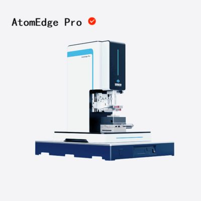
High-Stability AtomEdge Pro AFM: 4096×4096 Resolution 3D Scanning + EFM/KPFM/PFM
Product Description: The Atomic Force Microscope (AFM) is a cutting-edge instrument designed for high-precision surface analysis and nanoscale electrical measurement. Renowned for its versatility and advanced functionality, this AFM offers a comprehensive suite of features that make it an indispensable tool in both research and industrial applications. With a scanning rate adjustable between 0.1 and 30 Hz, users can tailor the imaging speed to suit a wide range of sample -

AtomEdge Pro: Multi-Functional Atomic Force Microscope – 3D Imaging For Materials
Product Description: The Atomic Force Microscope (AFM) is a cutting-edge instrument designed for high-precision surface analysis and characterization at the nanometer scale. This multifunctional measurement tool integrates several advanced microscopy techniques, including Electrostatic Force Microscopy (EFM), Scanning Kelvin Probe Microscopy (KPFM), Piezoelectric Force Microscopy (PFM), Magnetic Force Microscopy (MFM), and Force Curve measurements. These capabilities make it -
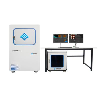
ميكروسكوب القوة الذرية على مستوى الوافر
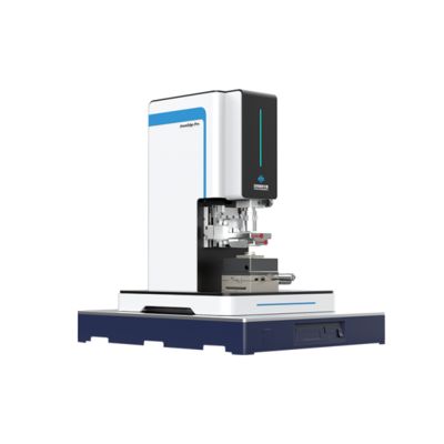
Wafer-Level Atomic Force Microscope Product Model: AtomMax Product Overview: Using micro-cantilever probe structures, this instrument enables 3D morphology characterization of conductive, semiconductive, and insulating solid materials, achieving wafer-level large-sample morphology characterization. Combined with an optical image, the electrically driven sample positioning stage allows for 1 μm positioning accuracy within a 200 x 200 mm area. with fully automated operations -
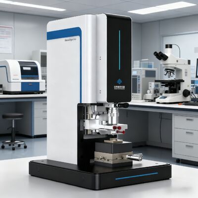
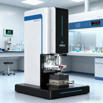
مجهر بيولوجي دقيق للمجهر الذري للقوة متعدد الوظائف
Multi-Functional Atomic Force Microscope Product Model: AtomEdge Pro Product Description: The AtomEdge Pro multi-functional atomic force microscope canperform three-dimensional scanning imaging on materials, electronic devices, biological samples, etc. lt features multiple working modes such as contact, tap, and non-contact, providing users with more flexible and precise operation options. In addition, it integrates multiple functional modes such as magnetic force microscopy, -
المجاهر الصناعية القابلة للتعديل بتقنية المجهر الذري للقوة ذات الإمكانات النانوية عالية الدقة
Nanoscale Potential With Atomic Force Microscope For High-Resolution Imaging Product Description: One of the key features of the AFM is its impressive scanning range, measuring at 100 μm X 100 μm X 10 μm. This wide range allows for detailed imaging and analysis of a variety of samples, from small nanoparticles to larger structures. With a scan speed ranging from 0.1Hz to 30Hz, the AFM offers versatility in capturing dynamic processes and obtaining quick results. Researchers


